Nikon Optiphot 100 Optical microscope
Nikon SMZ-2T Stereomicroscope
Nikon C1Si Confocal microscope
A scanning electron microscope (SEM) produces images of a sample by scanning the surface with a focused beam of electrons. The electrons interact with atoms in the sample, producing various signals that contain information about the surface topography and composition of the sample. In the most common SEM mode, secondary electrons emitted by atoms excited by the electron beam are detected using a secondary electron detector (Everhart–Thornley detector). The number of secondary electrons that can be detected, and thus the signal intensity, depends, among other things, on specimen topography. In a conventional SEM, the specimens are observed in high vacuum.
Energy-dispersive spectroscopy (EDS) is an analytical technique used for the elemental analysis or chemical characterisation of a sample. It relies on an interaction between a beam of electrons that is focused into the sample being studied, and the sample from which characteristic X-rays are emitted.
Equipment available:
Carl Zeiss Merlin Field Emission SEM
Ametek EDAX trident system

X-ray diffractometry (XRD) determines the atomic and molecular structure of a crystal, whereby the crystalline structure causes a beam of incident X-rays to diffract into many specific directions. By measuring the angles and intensities of these diffracted beams, the mean positions of the atoms in the crystal can be determined, as well as their chemical bonds, their crystallographic disorder, and various other information.
Equipment available:

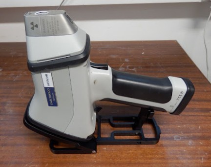
The Hitachi X-MET8000 Optimum is a handheld instrument that can analyse metals in a non-destructive way leaving no test mark. It emits X-rays which interact with the material and are reflected back into the instrument. From the analysis of the X-Rays reflected back, the instrument will provide a full chemical composition of the material being tested. Only a small area is needed to analyse the material. It is also equipped with a camera that keeps a record of the image of the surface being investigated. The software issues a report with all the measurements taken.
The Shimadzu Total Organic Carbon Analyser (Model: TOC-L CSN) is used for the measurement of dissolved organic and non-organic carbon in liquids using the 680°C combustion catalytic oxidation method combined with NDIR. It is used for the measurement of water quality. The total amount of all carbon present in water is referred to as “total carbon” (TC), which can be classified into two major types, either total organic carbon (TOC) or inorganic carbon (IC). Total organic carbon can be further classified as either non-purgeable organic carbon (NPOC) or purgeable organic carbon (POC).

Raman spectroscopy is a spectroscopic technique typically used to determine vibrational and rotational modes of molecules. Raman spectroscopy is commonly used in material analysis to provide a structural fingerprint by which molecules can be identified.
Equipment available:
The Shimadzu Spectrophotometer (Model: Solidspec-3700DUV) is a unique instrument for Malta. It can measure spectrums both in ambient air and also in inert gas. It can read over a wavelength range starting from 190 nm up to 3700 nm. It is equipped with an integrated sphere for the measurement of transmittance, specular reflectance, and diffused reflectance. It can also take measurements at different incident angles by varying the angle of the sample. It is used for both small samples and also for thin plates up to 250 mm x 250 mm.
Contact or non-contact profilometry is used to scan the topography of the surface on the micro scale. The roughness, curvature and flatness can then be measured.
Equipment available:
Atomic Force Microscopy (AFM) is primarily used to analyse the topography and surface properties of the samples on a nano scale. The information is gathered by "feeling" or "touching" the surface with a mechanical probe. Piezoelectric elements that facilitate tiny but accurate and precise movements on (electronic) command enable precise scanning.
Equipment available:

SPECS UHV Integrated Characterisation Chamber
RHK UHV Scanning Probe Microscopy Chamber

The DMME is equipped with a mobile Vacuum Leak Detector (Model: Pfeifer JSVA00A4MH9A [2019]). Using helium gas, the leak detector is capable of detecting leaks in installations that operate under vacuum conditions.
