A research project on energy harvesting electrical interfaces being carried out at the Department ofMicroelectronics and Nanoelectronics (MNE) by Inġ. Francarl Galea has been awarded a Hi-Silicon Sponsorship Program.
This sponsorship covers the costs of the fabrication of an integrated circuit prototype. This research project is focusing on the design of a power conditioning circuit for low power energy harvesting devices. The power conditioning circuit is compatible with various energy harvesting techniques such as piezoelectric, solar cells and thermoelectric energy harvesters.
Energy harvesters are devices which harvest energy from their surroundings in order to power small loads. These devices eliminate the need of using batteries in applications where the battery longevity is an issue and battery replacement might not be feasible.
A common disadvantage of energy harvesters is that their output is volatile and dependent on its current operating conditions. Thus, it is beneficial to have a power conditioning circuit to provide energy storage in order to minimize the downtime of the loads and a voltage regulation circuit to generate a constant output voltage. Energy harvesters also have an internal impedance and so it is beneficial for a power conditioning circuit to have a maximum power point tracking (MPPT) algorithm to match the load resistance to the internal impedance of the harvester by means of a switch-mode converter.
The designed power conditioning circuit consists of a full analogue MPPT circuit which controls an on-chip power circuit, capable to work both with an AC and a DC input voltage. Any excess power being generated by the energy harvester is stored in a high storage capacitor to guarantee longer operating times of the load. A hysteretic controlled regulating buck converter stage generates a clean constant output voltage as required by the load being connected.

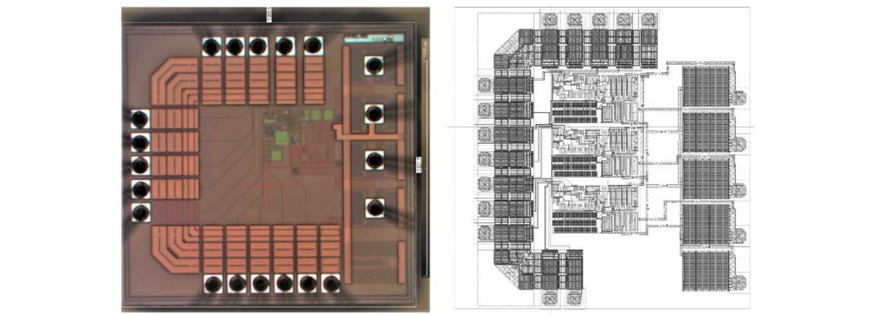
The first stage of the circuit is shown in Figure 1 (left) is the AC/DC-to-DC converter with MPPT control and this was already fabricated. The fabrication of the AC/DC-to-DC converter was funded by the ENDEAVOUR Scholarship Scheme (Malta). The scholarship is financed by National Fund. “Investing in human capital to create more opportunities and promote the wellbeing of society”. The voltage regulating stage shown in Figure 2 (right) uses a novel hysteretic control which features a low power consumption of around 500 nW. The control side (low voltage) is capacitively coupled to the bootstrapping power side (high voltage). This circuit is currently in the fabrication stage and the costs for this fabrication are being covered by the Hi-Silicon Sponsorship Program.


